Research by S M Hozaifa Hossain: devices that compute like brains.
Research
Ferroelectric FETs
TCAD & device physics
Spiking neural networks
Dhaka, Bangladesh
S M Hozaifa Hossain researches semiconductor devices and neuromorphic hardware: how ferroelectric transistors can act as low-energy synapses, and how TCAD, high-level synthesis and machine learning connect devices to algorithms. See also awards and publications.
Research · Thesis · CREST 2027
Undergraduate thesis · defended September 2026
What did my undergraduate thesis show?
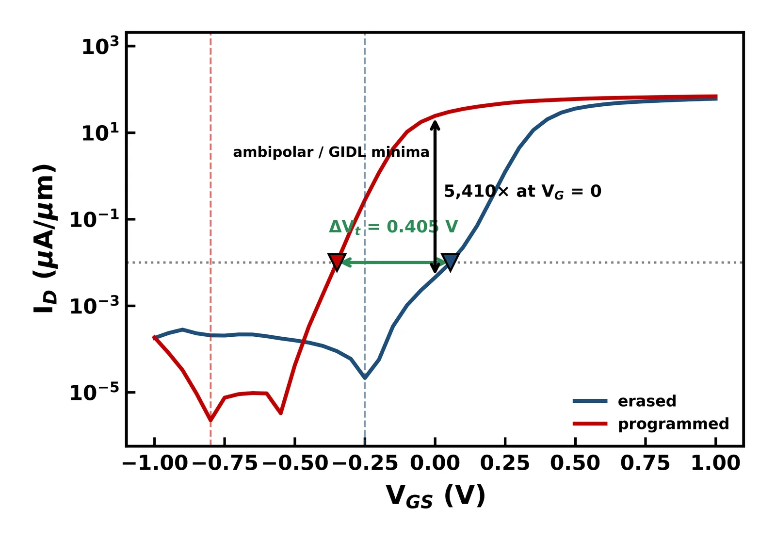
My thesis models a gate-all-around ferroelectric FET with a 7 nm HZO gate stack in Synopsys Sentaurus TCAD, then uses it as an artificial synapse in a spiking network. The device shows a 5410x memory window and a 63.5 mV/dec subthreshold slope, and the network classifies ECG heartbeats with 83.04% accuracy.
Title: Ferroelectric Gate-All-Around FETs for Next-Generation Neuromorphic Systems: Device Modeling and Spiking Network Implementation. Advisor: Dr. Mainul Hossain, University of Dhaka. The sub-100 nm device was calibrated with Preisach polarization dynamics against experimental data. Conductance-level placement mattered more to SNN accuracy than the number of levels. The calibrated conductance states were deployed in a PyTorch spiking recurrent network (SpikingJelly, leaky integrate-and-fire neurons) for 4-class arrhythmia classification on the MIT-BIH database.
Erased and programmed transfer curves: 5,410x at VGS = 0 V, retained ΔVT 0.405 V.
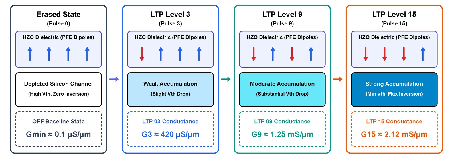
Channel conductance rises from the erased state to pulse 15 as HZO dipoles flip.
Key numbers
Memory window 5410x at VGS = 0 VRetained ΔVT 0.405 VSS 63.5 mV/dec<1% retention loss over 9.9e5 read cycles15 analog conductance states over 3.79 decades~9 aJ per switching pulse83.04% accuracy, macro-F1 0.75535.8 pJ per heartbeat
CREST 2027 · Silicon River Bangladesh
What is the CREST 2027 research project?
As a CREST 2027 Research Fellow at Silicon River Bangladesh, I will study how the curvature of the channel limits the number of reliable analog states in gate-all-around FeFET synapses. The study combines Sentaurus TCAD simulation with machine learning. A synapse that holds more distinguishable conductance levels stores more weights per device, so the question is where the geometry sets a ceiling.
The fellowship runs January to December 2027 at the Center for Research Excellence on Semiconductor Technology, supported by Neural Semiconductor Ltd. It builds on the thesis, where 15 analog conductance states were extracted for a GAA device and a planar reference supported 10. My advisor is Dr. Mainul Hossain.
Fellowship
Selected 30 October 2026Fellowship: Jan to Dec 2027Advisor: Dr. Mainul HossainHost: Silicon River Bangladesh
IEEE EDS TCAD Hackathon 2026
How does stress improve a sub-10 nm gate-all-around nanowire transistor?
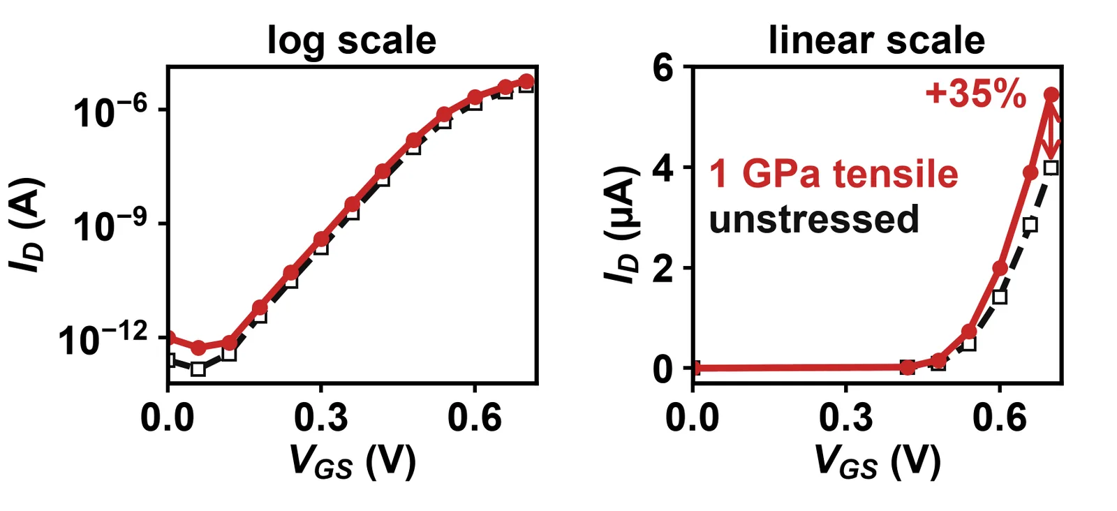
Applying 1 GPa of uniaxial tensile stress along a 6 nm silicon nanowire repopulates its conduction-band subbands. In my Sentaurus TCAD design this gave 35% more on-current and 32% more transconductance, while band-to-band tunneling and quantum corrections kept off-state leakage at 0.99 pA.
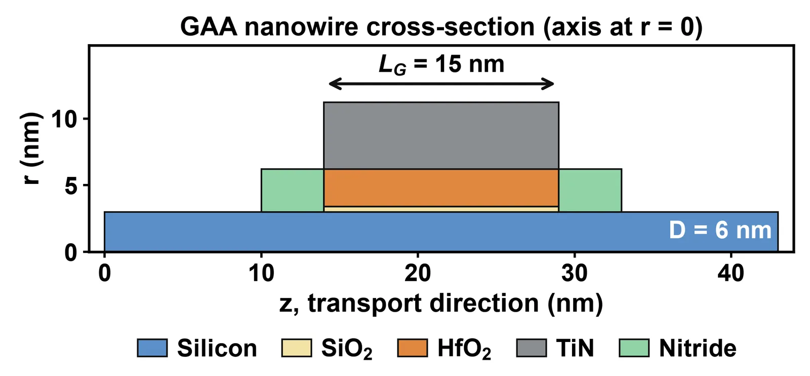
The nMOS has a 15 nm gate length, 6 nm diameter and 0.9 nm EOT (0.4 nm SiO2 interface layer plus 2.82 nm HfO2, κ = 22), built as a six-material 3D cylinder in Sentaurus Structure Editor with 0.2 nm radial mesh refinement. Simulation used deformation-potential and eSubBand models, density-gradient quantum correction and nonlocal-path band-to-band tunneling. This design made me one of three international winners of the IEEE EDS TCAD Hackathon 2026, and the first winner from Bangladesh.
Drain current with and without 1 GPa tensile stress: +35% ION.
Key numbers
+35% ION (5.42 µA, 287 µA/µm)+32% gm (2.10 mS/µm)IOFF 0.99 pA, ION/IOFF 5.5e6SS 61 mV/dec at VDD 0.7 V
Tesseract Hackathon 2026 · Best-in-Track
What is Differentiable Silicon?
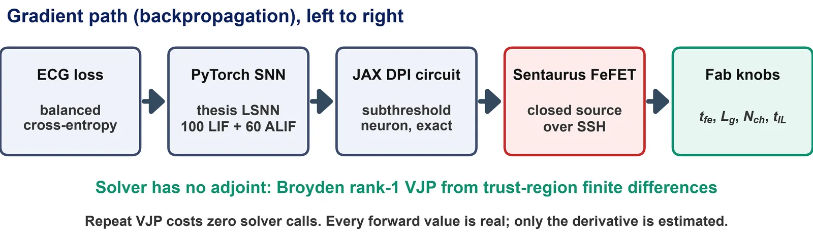
Differentiable Silicon is a pipeline that passes one gradient from an ECG classification loss through a PyTorch spiking network and a JAX device-to-neuron model into Synopsys Sentaurus TCAD. That tells you how four FeFET fabrication parameters should change to improve accuracy, even though the TCAD solver is a closed binary.
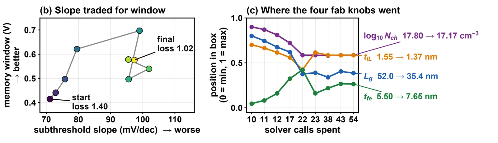
The closed solver has no adjoint, so the missing gradient was manufactured with trust-region finite-difference probes and a Broyden update. Descent cut balanced cross-entropy from 1.400 to 1.018 and raised accuracy from 0.250 to 0.688 in 64 solver calls. It won Best-in-Track in the Hybrid ML x Mechanistic Models track, run by Pasteur Labs and ISI.
Gradient path from the ECG loss back to four fabrication parameters. The solver has no adjoint, so the last step is estimated.
How the memory window and slope traded off, and where the four parameters moved.
Key numbers
4 FeFET fabrication parametersCross-entropy 1.400 to 1.018Accuracy 0.250 to 0.68864 solver calls
Siemens EDA HLS Hackathon 2026 · 1st place
How was a CNN accelerator made 915 times more energy efficient?
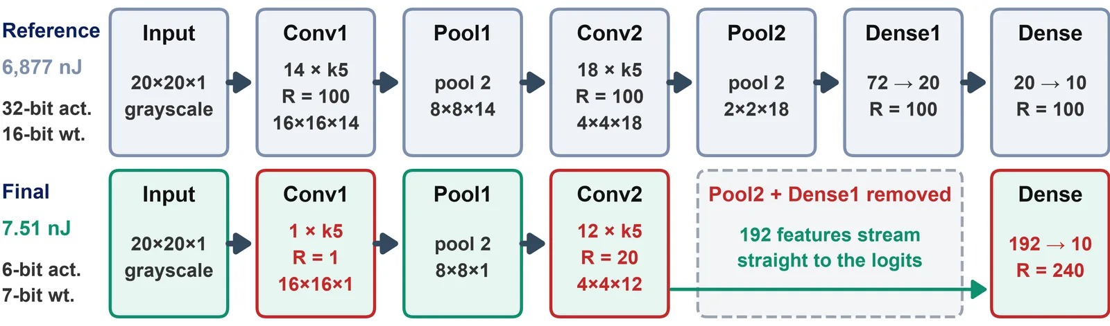
I designed an ultra-low-power CNN accelerator for roadside-object recognition by exploring many high-level synthesis configurations, then measuring real gate-level power. Energy per inference fell from 6,877 nJ to 7.51 nJ, a 915x reduction, at 95.3% accuracy. The result took first place in the Siemens EDA hackathon.
The flow used QKeras and hls4ml to move the quantized network into Siemens Catapult HLS, targeted a 45 nm ASIC library, and measured power with PowerPro at gate level. The final design came from 365 synthesis runs.